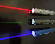


 الفيزياء الكلاسيكية
 الكهربائية والمغناطيسية
 علم البصريات
 الفيزياء الحديثة
 النظرية النسبية
 الفيزياء النووية
 فيزياء الحالة الصلبة
 الليزر
 علم الفلك
 المجموعة الشمسية
 الطاقة البديلة
 الفيزياء والعلوم الأخرى
 مواضيع عامة في الفيزياء
|
Read More
Date: 21-10-2020
Date: 14-5-2017
Date: 18-10-2020
|
Epitaxial Growth
A common and versatile growth technique that is used extensively in device and integrated circuit fabrication is epitaxial growth. Epitaxial growth is a process whereby a thin, single-crystal layer of material is grown on the surface of a single-crystal substrate.
In the epitaxial process, the single-crystal substrate acts as the seed, although the process takes place far below the melting temperature. When an epitaxial layer is grown on a substrate of the same material, the process is termed heteroepitaxy. Growing silicon on a silicon substrate is one example of a heteroepitaxy process. At present, a great deal of work is being done with heteroepitaxy. In a heteroepitaxy process, although the substrate and epitaxial materials are not the same, the two crystal structures should be very similar if single-crystal growth is to he obtained and if a large number of defects are to be avoided at the epitaxial-substrate interface. Growing epitaxial layers of the ternary alloy AlGaAs on a GaAs substrate is one example of a heteroepitaxy process.
One epitaxial growth technique that has been used extensively is called chemical vapor-phase deposition (CVD). Silicon epitaxial layers, for example, are grown on silicon substrates by the controlled deposition of silicon atoms onto the surface from a chemical vapor containing silicon. In one method, silicon tetrachloride reacts with hydrogen at the surface of a heated substrate. The silicon atoms are released in the reaction and can be deposited onto the substrate, while the other chemical reactant, HCI, is in gaseous form and is swept out of the reactor. A sharp demarcation between the impurity doping in the substrate and in the epitaxial layer can be achieved using the CVD process. This technique allows great flexibility in the fabrication of semiconductor devices.
Liquid-phase epitaxy is another epitaxial growth technique. A compound of the semiconductor with another element may have a melting temperature lower than that of the semiconductor itself. The semiconductor substrate is held in the liquid compound and, since the temperature of the melt is lower than the melting temperature of the substrate, the substrate does not melt. As the solution is slowly cooled, a single crystal semiconductor layer grows on the seed crystal. This technique, which occurs at a lower temperature than the Czochralski method, is useful in growing group Ill-V compound semiconductors.
A versatile technique for growing epitaxial layers is the molecular beam epitaxy (MBE) process. A substrate is held in vacuum at a temperature normally in the range of 400 to 800oC, a relatively low temperature compared with many semiconductor processing steps. Semiconductor and dopant atoms are then evaporated onto the surface of the substrate. In this technique, the doping can he precisely controlled resulting in very complex doping profiles. Complex ternary compounds, such as AlGaAs, can be grown on substrates, such as GaAs, where abrupt changes in the crystal composition are desired. Many layers of various types of epitaxial compositions can be grown on a substrate in this manner. These structures are extremely beneficial in optical devices such as laser diodes.


|
|
|
|
تفوقت في الاختبار على الجميع.. فاكهة "خارقة" في عالم التغذية
|
|
|
|
|
|
|
أمين عام أوبك: النفط الخام والغاز الطبيعي "هبة من الله"
|
|
|
|
|
|
|
قسم شؤون المعارف ينظم دورة عن آليات عمل الفهارس الفنية للموسوعات والكتب لملاكاته
|
|
|