آخر المواضيع المضافة

 الفيزياء الكلاسيكية
الكهربائية والمغناطيسية
علم البصريات
الفيزياء الحديثة
النظرية النسبية
الفيزياء النووية
فيزياء الحالة الصلبة
الليزر
علم الفلك
المجموعة الشمسية
الطاقة البديلة
الفيزياء والعلوم الأخرى
مواضيع عامة في الفيزياء
الفيزياء الكلاسيكية
الكهربائية والمغناطيسية
علم البصريات
الفيزياء الحديثة
النظرية النسبية
الفيزياء النووية
فيزياء الحالة الصلبة
الليزر
علم الفلك
المجموعة الشمسية
الطاقة البديلة
الفيزياء والعلوم الأخرى
مواضيع عامة في الفيزياء| Semiconductors |


|
|
Read More
Date: 28-10-2020
Date: 18-10-2020
Date: 17-5-2017
|
Semiconductors
In some solids silicon and germanium are important examples the situation arises where band B is full but band A is very close to it. In terms of our discussion about insulators, such a solid should not carry an electric current since the band B is full. However, because band A is very close to band B, electrons from B can sometimes jump into A because of the energy they can acquire from thermal excitation. Clearly, the higher the tempera ture the higher the thermal energy of the electrons and the more likely they are to jump into band A. This band will not have the full complement of electrons allowed by the exclusion principle and therefore behaves as a conduction band so that an electric current can pass. Such a solid, because it can carry a current by this means, is referred to as a semiconductor. Its conductivity is much lower than that of a metal because there are far fewer electrons participating. The conductivity is also very dependent on temperature and a semiconductor resistance can decrease by a factor of around two for every ten degree temperature rise. Its conductivity can also be increased by shining light onto it, the photons in the light giving energy to electrons in band B, enabling them to jump into band A. Such a semiconductor is referred to as a photoconductor. However, the most effective way of increasing the conductivity of a semiconductor is to ‘dope’ it with an impurity, Consider the semiconductor germanium with a small amount of arsenic as an impurity. The arsenic atom is very similar to germanium except that it has an additional electron. If a germanium atom is replaced by an arsenic atom in a germanium crystal then there is a spare electron. It turns out that the energy level of this electron is just below the bottom of the band A as shown in figure 1.1(a). Its energy level is so close to this band that, unless the temperature is very low indeed, thermal energy is enough to cause it to jump into the band and therfore act as a conduction electron. Impurities of a
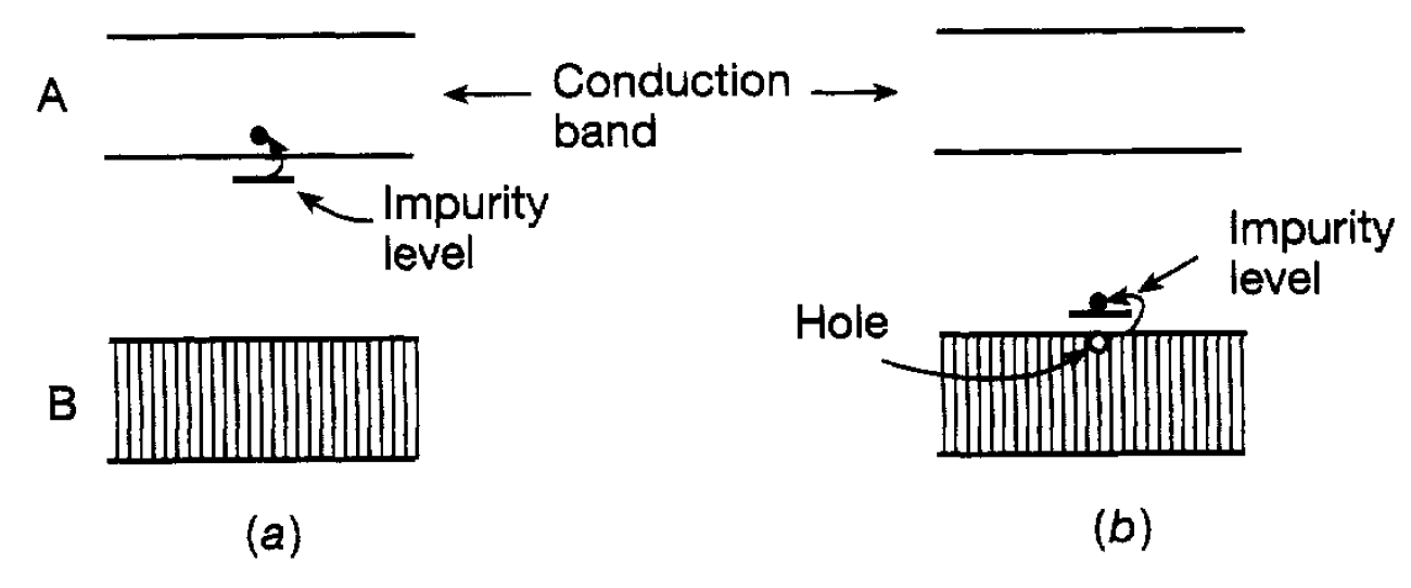
Figure 1.1: Semiconductor band structures: (a) a donor impurity; (b) an acceptor impurity.
few parts in a million are sufficient to provide a very large number of conduction electrons and can lead to a thousandfold increase in the conductivity. Since the impurity donates electrons it is known as a donor impurity and, because the current is carried by these (negatively charged) electrons, the doped germanium is referred to as an n-type semiconductor. Another way to increase the conductivity, of germanium is to introduce the impurity gallium. The gallium atom has one electron less than germanium and when introduced as an impurity there is an impurity energy level available for an electron just above the band B as shown in figure 1.1(b). This means that, because of its thermal energy, an electron from the band B can jump into this level leaving, as it were, a ‘hole’ in the band. When an electric field is applied another nearby electron in band B can jump into the hole and this process can continue so that the hole moves steadily through the germanium under the influence of the electric field. This is another form of electric current since electric charge is being displaced through the solid. An impurity of this form is referred to as an acceptor impurity since an electron from the band B is accepted into an empty energy level due to the impurity. Also since the hole travels in the opposite direction to the electrons it behaves as though it had a positive charge and we now speak of a p-type semiconductor. Both n-type and p-type semiconductors play a profound role in the construction of all electronic apparatus from transistor radios, television and pocket calculators through to computer systems at all levels of scale. The basic ingredient is the p-n junction (referred to as a diode) consisting of p-type and n-type semiconductor layers in contact with each other as in figure 1.2(a). This can be arranged within the same crystal-usually silicon or germanium. It is found that with such an arrangement electrons can be drawn through it if the positive pole of the battery is connected to the player and the negative pole to the n-layer. Roughly speaking, electrons are continually ‘pumped’ into the n-region and removed from the p-region, this latter process being equivalent to pumping ‘holes’ into that region. However, if the battery is connected the other way round electrons are ‘sucked out’ of the n-region and holes out of the p-region. The carriers of electricity are therefore
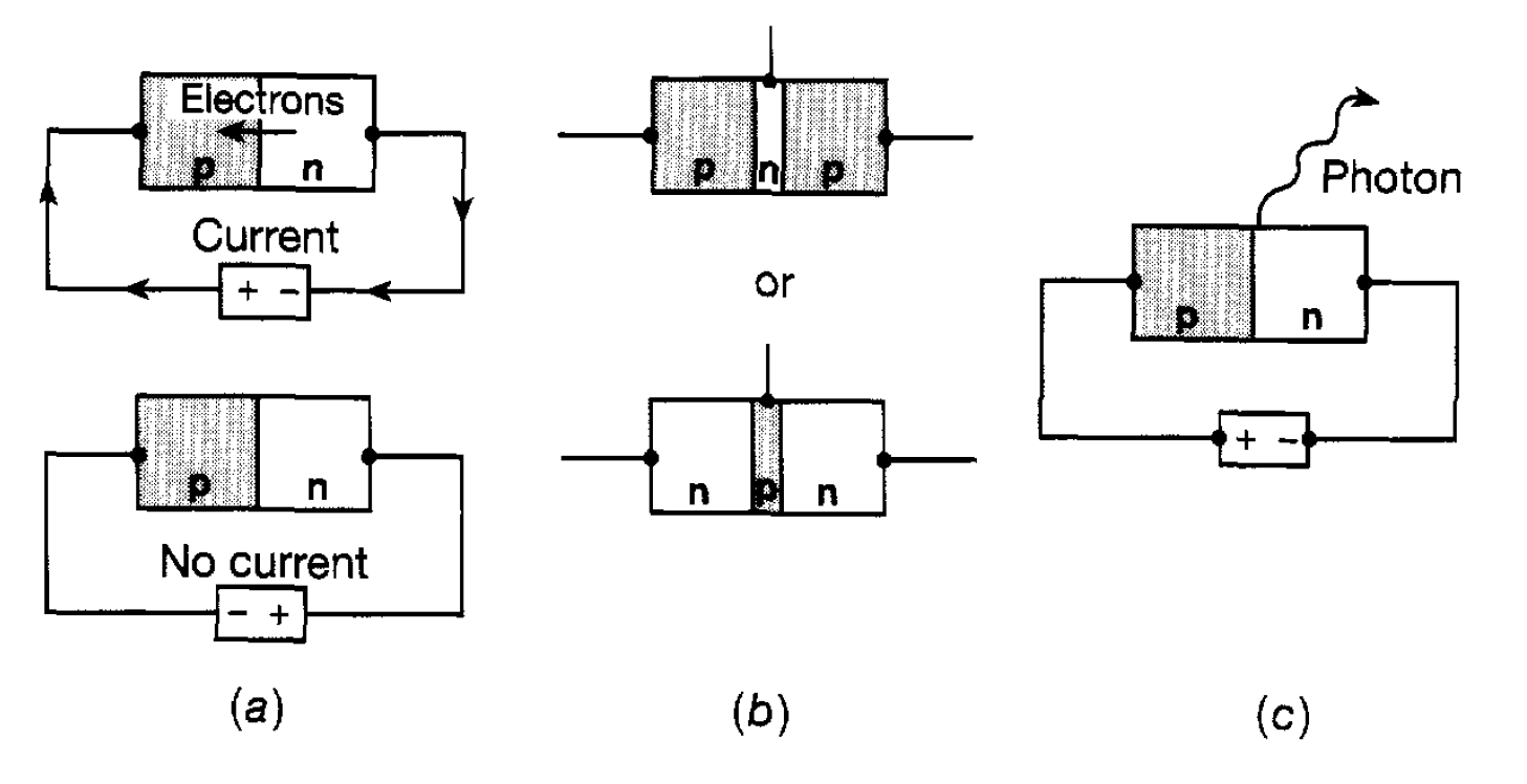
Figure 1.2: Semiconductor devices: (a) a diode; (b) a transistor; (c) an LED.
removed and the flow of electricity stops. Such an arrangement therefore allows an electric current to flow one way but not the other. A more complex arrangement is to have a n-p-n or a p-n-p junction with a thin middle region as in figure 1.2(b). This is known as a transistor (or a triode) and has the property that the electric potential on the middle section can be used to control the flow of current through the device. This enables, for example, a weak electrical signal being fed to the middle section to cause a large change in the current through the device and hence to amplify the signal. As a current flows through a p-n junction electrons frequently fall into holes. Both obviously disappear and energy is released. In some materials this energy is sufficiently large to lead to the emission of a visible photon (see figure 1.2(c)). This is the basis of operation of LEDs (light emitting diodes) which are used in the visual displays of many electronic devices. Conversely, by shining light onto such a junction, electrons can be excited into the conduction band and these, together with the resultant holes, lead to flow of current if an external circuit is connected. This is the mechanism underlying the functioning of solar cells used for the generation of electricity, for example, in satellites. Associated with the development of diodes, transistors etc are the techniques of miniaturization. These allow many semiconductor components of the above kind to be connected together in an extremely small space within the same crystal. It is possible to incorporate very complicated circuits inolving literally tens of thousands of such components on thin wafers of material with areas of the order of one square centimetre or less. These are referred to as integrated circuits and the wafer containing them as a chip, often called a silicon chip. That such complex circuits can be contained in such a small space has two benefits. First it has enabled the construction of very small but highly sophisticated electronic devices of which the pocket calculator and the digital watch are common examples. Second, because the chips are so small, signals between the different components can move very quickly, , so enabling the development of high speed large scale computers.

|
|
|
|
التوتر والسرطان.. علماء يحذرون من "صلة خطيرة"
|
|
|
|
|
|
|
مرآة السيارة: مدى دقة عكسها للصورة الصحيحة
|
|
|
|
|
|
|
نحو شراكة وطنية متكاملة.. الأمين العام للعتبة الحسينية يبحث مع وكيل وزارة الخارجية آفاق التعاون المؤسسي
|
|
|