

 الفيزياء الكلاسيكية
 الكهربائية والمغناطيسية
 علم البصريات
 الفيزياء الحديثة
 النظرية النسبية
 الفيزياء النووية
 فيزياء الحالة الصلبة
 الليزر
 علم الفلك
 المجموعة الشمسية
 الطاقة البديلة
 الفيزياء والعلوم الأخرى
 مواضيع عامة في الفيزياء
|
Read More
Date: 22-10-2020
Date: 8-5-2017
Date: 18-10-2020
|
Growth from a Melt
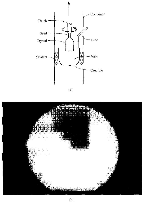
A common technique for growing single-crystal materials is called the Czochralski method. In this technique, a small piece of single-crystal material, known as a seed, is brought into contact with the surface of the same material in liquid phase, and then slowly pulled from the melt. As the seed is slowly pulled, solidification occurs along the plane between the solid-liquid interface. Usually the crystal is also rotated slowly as it is being pulled, to provide a slight stirring action to the melt, resulting in a more uniform temperature. Controlled amounts of specific impurity atoms, such as boron or phosphorus, may be added to the melt so that the grown semiconductor crystal is intentionally doped with the impurity atom. Figure 1.1 shows a schematic of the Czochralski growth process and a silicon ingot or boule grown by this process.

Figure 1.1 (a) Model of a crystal puller and (b) photograph of a silicon wafer with an array of integrated circuits. The circuits are tested on the wafer then sawed apart into chips that are mounted into packages. (Photo courtesy of Intel Corporation.)
Some impurities may be present in the ingot that are undesirable. Zone refining is a common technique for purifying material. A high-temperature coil. or r-f induction coil, is slowly passed along the length of the boule. The temperature induced by the coil is high enough so that a thin layer of liquid is formed. At the solid-liquid interface, there is a distribution of impurities between the two phases. The parameter that describes this distribution is called the segregation coefficient: the ratio of the concentration of impurities in the solid to the concentration in the liquid. If the segregation coefficient is 0.1, for example, the concentration of impurities in the liquid is a factor of 10 greater than that in the solid. As the liquid zone moves through the material. the impurities are driven along with the liquid. After several passes of the r-f coil, most impurities are at the end of the bar, which can then be cut off. The moving molten zone, or the zone-refining technique, can result in considerable purification.
After the semiconductor is grown, the boule is mechanically trimmed to the proper diameter and a Rat is ground over the entire length of the boule to denote the crystal orientation. The Rat is perpendicular to the [110] direction or indicates the (110) plane. (See Figure 1.1b.) This then allows the individual chips to be fabricated along given crystal planes so that the chips can he sawed apart more easily. The boule is then sliced into wafers. The wafer must he thick enough to mechanically support itself. A mechanical two-sided lapping operation produces a Rat wafer of uniform thickness. Since the lapping procedure can leave a surface damaged and contaminated by the mechanical operation, the surface must be removed by chemical etching. The final step is polishing. This provides a smooth surface on which devices may be fabricated or further growth processes may be carried out. This final semiconductor wafer is called the substrate material.


|
|
|
|
دراسة: حفنة من الجوز يوميا تحميك من سرطان القولون
|
|
|
|
|
|
|
تنشيط أول مفاعل ملح منصهر يستعمل الثوريوم في العالم.. سباق "الأرنب والسلحفاة"
|
|
|
|
|
|
|
تثميناً لجهودهم.. العتبة العباسية المقدسة تكرِّم اللجنة التحكيمية والجهات المساهمة بمسابقة فنِّ الخطابة
|
|
|