تاريخ الفيزياء
علماء الفيزياء


الفيزياء الكلاسيكية
الميكانيك
الديناميكا الحرارية
الكهربائية والمغناطيسية
الكهربائية
المغناطيسية
الكهرومغناطيسية
علم البصريات
تاريخ علم البصريات
الضوء
مواضيع عامة في علم البصريات
الصوت
الفيزياء الحديثة
النظرية النسبية
النظرية النسبية الخاصة
النظرية النسبية العامة
مواضيع عامة في النظرية النسبية
ميكانيكا الكم
الفيزياء الذرية
الفيزياء الجزيئية
الفيزياء النووية
مواضيع عامة في الفيزياء النووية
النشاط الاشعاعي
فيزياء الحالة الصلبة
الموصلات
أشباه الموصلات
العوازل
مواضيع عامة في الفيزياء الصلبة
فيزياء الجوامد
الليزر
أنواع الليزر
بعض تطبيقات الليزر
مواضيع عامة في الليزر
علم الفلك
تاريخ وعلماء علم الفلك
الثقوب السوداء
المجموعة الشمسية
الشمس
كوكب عطارد
كوكب الزهرة
كوكب الأرض
كوكب المريخ
كوكب المشتري
كوكب زحل
كوكب أورانوس
كوكب نبتون
كوكب بلوتو
القمر
كواكب ومواضيع اخرى
مواضيع عامة في علم الفلك
النجوم
البلازما
الألكترونيات
خواص المادة
الطاقة البديلة
الطاقة الشمسية
مواضيع عامة في الطاقة البديلة
المد والجزر
فيزياء الجسيمات
الفيزياء والعلوم الأخرى
الفيزياء الكيميائية
الفيزياء الرياضية
الفيزياء الحيوية
الفيزياء والفلسفة
الفيزياء العامة
مواضيع عامة في الفيزياء
تجارب فيزيائية
مصطلحات وتعاريف فيزيائية
وحدات القياس الفيزيائية
طرائف الفيزياء
مواضيع اخرى

How the junction works
 المؤلف:
Stan Gibilisco
المؤلف:
Stan Gibilisco
 المصدر:
Teach Yourself Electricity and Electronics
المصدر:
Teach Yourself Electricity and Electronics
 الجزء والصفحة:
364
الجزء والصفحة:
364
 5-5-2021
 2445
2445


+
-
20
How the junction works
When the N-type material is negative with respect to the P-type, electrons flow easily from N to P. The N-type semiconductor, which already has an excess of electrons, gets even more; the P-type semiconductor, with a shortage of electrons, is made even more deficient. The N-type material constantly feeds electrons to the P-type in an attempt to create an electron balance, and the battery or power supply keeps robbing electrons from the P-type material. This is shown in Fig. 1A and is known as forward bias.
When the polarity is switched so the N-type material is positive with respect to the P type, things get interesting. This is called reverse bias. Electrons in the N-type material
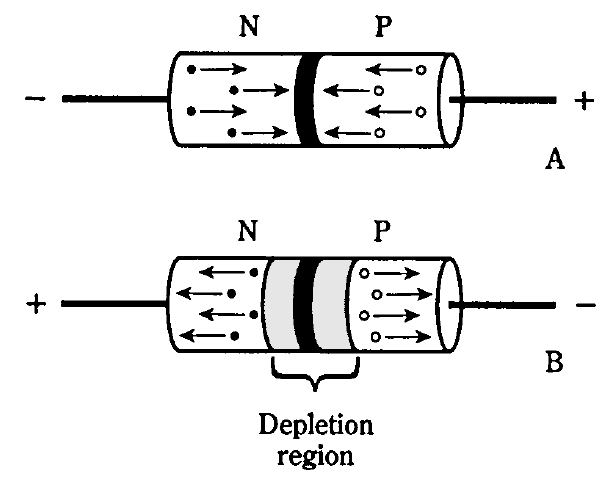
Fig. 1: At A, forward bias of a P-N junction; at B, reverse bias. Electrons are shown as small dots, and holes are shown as open circles.
are pulled towards the positive charge, away from the junction. In the P-type material, holes are pulled toward the negative charge, also away from the junction. The electrons (in the N-type material) and holes (in the P type) are the majority charge carriers. They become depleted in the vicinity of the P-N junction (Fig. 1B). A shortage of majority carriers means that the semiconductor material cannot conduct well. Thus, the depletion region acts like an insulator.
 الاكثر قراءة في الألكترونيات
 اخر الاخبار
اخبار العتبة العباسية المقدسة

الآخبار الصحية


مواضيع ذات صلة
 قسم الشؤون الفكرية يصدر كتاباً يوثق تاريخ السدانة في العتبة العباسية المقدسة
 "المهمة".. إصدار قصصي يوثّق القصص الفائزة في مسابقة فتوى الدفاع المقدسة للقصة القصيرة
 (نوافذ).. إصدار أدبي يوثق القصص الفائزة في مسابقة الإمام العسكري (عليه السلام)